
#612 Hi-Lo Logic Tester Kit
Building a neat little hi/low logic indicator kit using a CD4511 and a few passives; also fixing a circuit bug that prevents the power indicator from working.

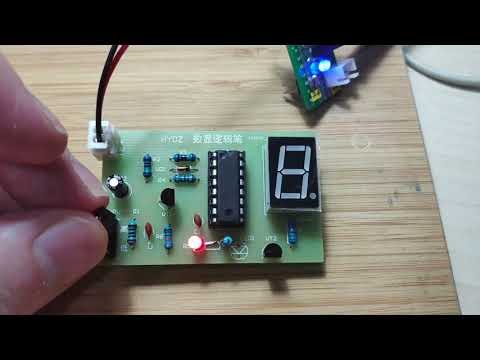
Here’s a quick demo..
Notes
This is cheap little kit that one might want to pick up for a few reasons:
- good for some through-hole soldering practice
- learn about the interesting CD4511 BCD-to-7 Segment Latch/Decoder/Driver
- study the neat trick used to get a “H” or “L” indicator with just a few passive components
Kit and Parts

| Ref | Item | Description |
|---|---|---|
| R1 | 2kΩ | |
| R2 | 1MΩ | |
| R3 | 1MΩ | |
| R4 | 120kΩ | |
| R5 | 1kΩ | |
| R6 | 10kΩ | |
| R7 | 51Ω | |
| C1 | 221 - 220pF | |
| C2 | 4.7µF | |
| C3 | 473 - 47nF | |
| VD1 | 1N4148 | |
| LED1 | 5mm Red LED | |
| LED2 | 7-segment | 5161AH |
| U1 | CD4511 | |
| VT1 | 9014 NPN | |
| VT2 | 9014 NPN | |
| 4-pin header | for probe input | |
| 2 wires | for power - unused, I replaced with XH2.54 connector |
Principle of Operation
The input level varies the B, C and !BLK values according to the following table:
| INPUT | D | C | B | A | LE | !BLK | !LT | 7-Seg Char |
|---|---|---|---|---|---|---|---|---|
| (float) | 0 | 0 | x | 0 | 0 | 0 | 1 | (blank) |
| low | 0 | 1 | 0 | 0 | 0 | 1 | 1 | 4 |
| high | 0 | 1 | 1 | 0 | 0 | 1 | 1 | 6 |
When input floating:
- VT1 base pulled high, which pulls C and !BLK low
- since !BLK low, no 7-segment output regardless of other input
When input high:
- VT1 base pulled high, but also VT1 collector via VD1, hence C and !BLK pulled high
- B pulled high via R2
- sets DCBA = 0110 i.e. 4511 output “6”,
- the 4511 Output maps to the 7-segment elements a-g as follows. i.e. displays “H”:
| 4511 Output | a | b | c | d | e | f | g |
|---|---|---|---|---|---|---|---|
| a : 0 (n/c) | |||||||
| b : 0 | 0 | ||||||
| c : 1 (n/c) | |||||||
| d : 1 | 1 | 1 | |||||
| e : 1 | 1 | ||||||
| f : 1 | 1 | ||||||
| g : 1 | 1 |
When input low:
- VT1 base pulled low (off), hence C and !BLK pulled high
- B pulled low via C3
- sets DCBA = 0100 i.e. 4511 output “4”,
- the 4511 Output maps to the 7-segment elements a-g as follows. i.e. displays “L”:
| 4511 Output | a | b | c | d | e | f | g |
|---|---|---|---|---|---|---|---|
| a : 0 (n/c) | |||||||
| b : 1 | 1 | ||||||
| c : 1 (n/c) | |||||||
| d : 0 | 0 | 0 | |||||
| e : 0 | 0 | ||||||
| f : 1 | 1 | ||||||
| g : 1 | 1 |
Original Schematic
Here’s the schematic for the board I received. Note however:
- there are a few variations of the schematic floating around, perhaps even difference PCB designs from different vendors
- the red LED1 is intended to be a power indicator, but it never turns on. There is a simple fix however - see the next section.

As build per the kit and original schematic. It works, just without the power indicator.
Input “LOW”:

Input “HIGH”:

Modified Schematic
Here’s a redrawing and modification to circuit to allow the LED1 power indicator to work correctly. Essentially:
- PCB LED1 footprint not populated (open circuit)
- LED1 and R5 connected in series in the PCB footprint provided for R5
- end result - LED is in the pull-up connection for VT2 base. So as long as there is enough power to enable the circuit, LED1 will light.


Input not connected/floating:

Input “LOW”:

Input “HIGH”:
