#217 Basic AVR-controlled Buck Converter
A simple buck converter circuit from first principles.
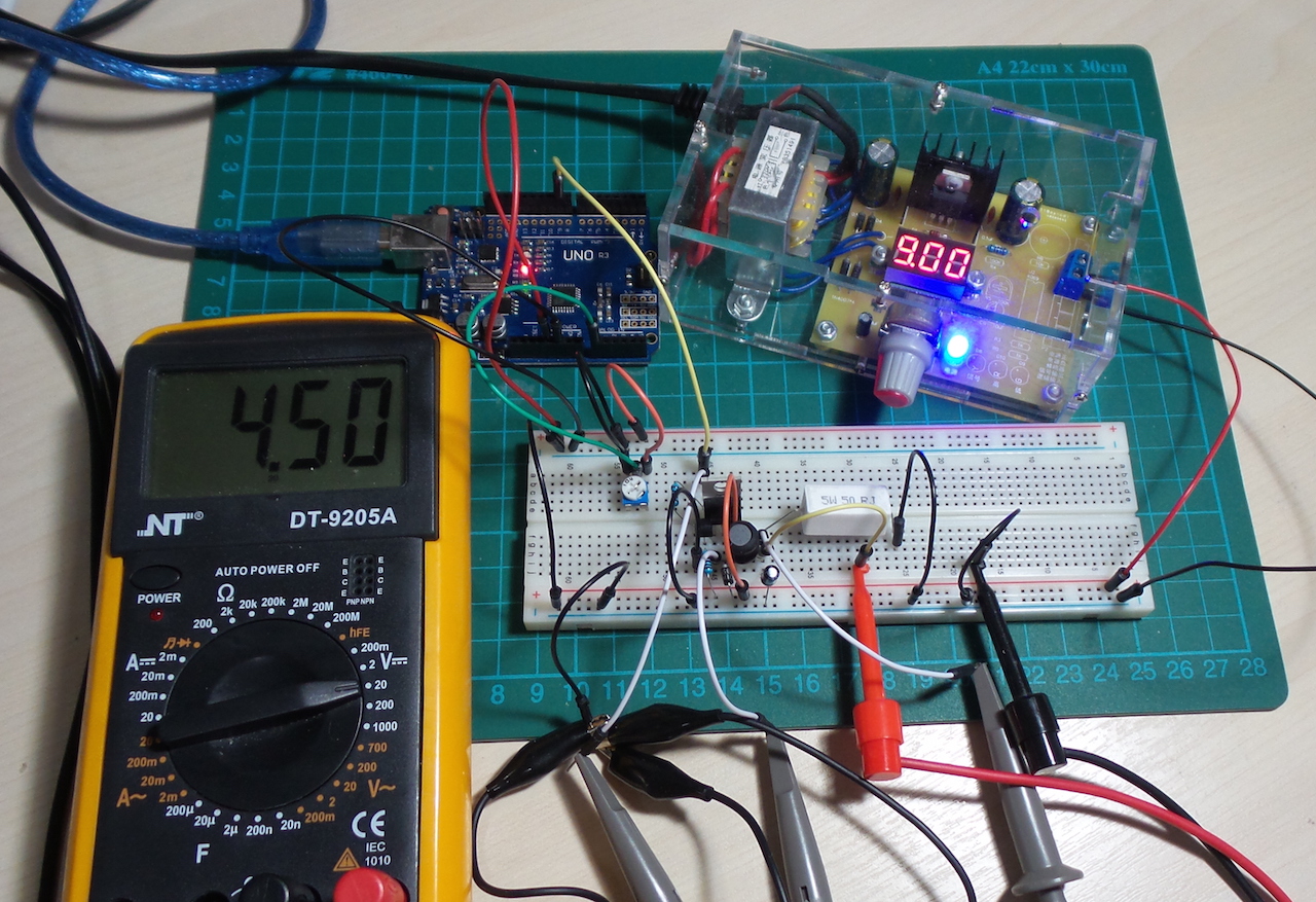
Notes
Buck converters are switching power supplies configured such that the output voltage is lower than the input voltage.
Since the primary components (inductor and capacitor) ideally consume no power, high conversion efficiencies are possible. In practice of course, components are not ideal and there is some power loss. More significant however is any power consumed in the control and feedback circuits.
This circuit is a demonstration and exploration of the basic buck configuration with a fixed load. Since the load is fixed, I have not implemented any feedback control system. Of course there are plenty of buck converter chips and modules on the market and these are so cheap you’d be crazy (or have such precise and unusual requirements) to build your own for a real application. But it’s nice to see how they work!
My inspiration for this circuit was DIY Buck Converter by GreatScott! - IMHO the “missing lab” to accompany very good but dry courses such as the Power Electronics Specialization from University of Colorado Boulder.
Operating Principle
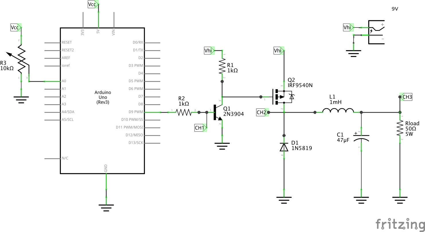
This is the basic buck:
- when the switch is on, current rises in the inductor to primarily charge the capacitor
- when the switch is off, stored energy in the inductor shunted to the capacitor/load. When depleted, the capacitor discharges into the load (reverse current prevented by the diode)
The inductor and capacitor effectively act as a low pass filter on the switching input. For good performance, it is therefore necessary for the switching frequency to be higher than the corner frequency of the filter.
Since the load is part of the circuit, actual output voltage performance is a function of all components:
- input voltage
- switching frequency
- actual load, inductor and capacitor values
PWM Generation
An Arduino is used to generate the switching signal using PWM output. The standard PWM frequency on a 16MHz core is 488 Hz, which is too low to achieve anything like a smooth output voltage. The PwmFrequency function is used to help set the PWM frequency scalars.
I’m using pin 9 for PWM output, at the highest possible frequency of 31250 Hz. I chose pin 9 as it uses timer1, so avoids conflicts with standard timer functions (I’m using FlexiTimer2 in this sketch).
The adjustment() function runs periodically to set the PWM frequency according to the potentiometer input.
Switch Control
The circuit is switched using a high-side p-channel MOSFET (IRF9540N). The FET switches:
- OFF when the gate-source voltage is below threshold voltage (-2V to -4V for the IRF9540N)
- ON when the gate-source voltage is above the threshold voltage
With 9V supply (source), there for the gate voltage needs to swing above 7V and below 5V for hard off and on.
Since these voltages are outside what Arduino GPIO pins can handle - see Method #3: Apply Over-voltage to I/O Pins for what happens if you do - an intermediate switching stage is required.
Although not the most efficient, I’m using a 2N3904 NPN transistor for this. The PWM output switches the 2N3904 in a 5V range, which in turn switches the IRF9540N which controls the input power supply (9V in my case, but could be higher).
When the 2N3904 is off, the collector-side resistor pulls the IRF9540N gate high (off).
It’s necessary to ensure the 2N3904 gets far enough into saturation to pull IRF9540N gate low enough. Quick calcs with a 1kΩ base resistor Ibe = 4.05mA:
Ibe = (V - Vbe) / Rb
Ibe = (5V - 0.95V) / 1000Ω
This puts the the transistor well into collector saturation. Assuming a worst-case ß/hFE of 30, the Ic collector can sink in excess of 100mA.
With 1kΩ collector resistor, and Vce(sat) of 0.2V, collector current will be ~8.8mA, so definitely on.
Note that throttling the collector current with a higher resistor can cut the power wastage, but going too low has an adverse impact on the switching time, and the IRF9540N never saturating.
Theoretical Performance
Terms:
- Vg = input voltage
- V = output voltage (average)
- D = duty cycle (%)
- T = switching period = 1/f
- f = switching frequency
- L = inductance
- C = capacitance
Inductor current is estimated with the small-ripple approximation.
First interval (switch on) of period D.Ts, change in inductor current il(t):
dil(t)/dt = (Vg - V) / L
Second interval (switch off) of period (1-D).Ts, change in inductor current il(t):
dil(t)/dt = - V / L
Inductor current ripple ilr:
ilr = (Vg - V) * D * T / (2 * L)
Inductor volt-second balance dictates average inductor voltage is 0 in steady-state, therefore output voltage V:
(Vg - V) * DT = V * (1-D) * T
V = D * Vg
Since we also require capacitor charge-balance, and assuming all inductor current ripple goes to capacitor,
then the capacitor voltage ripple vcr:
vcr = ilr * T / (8 * C)
So for the 50% duty cycle situation, theoretical performance ignoring real component loses and behaviours is as follows:
L = 1mH
C = 47µF
Vg = 9V
f = 31250 Hz
T = 32µs
D = 50%
Calculated output voltage = 4.5V:
V = D * Vg
Calculated inductor current ripple ilr = 36mA:
ilr = (Vg - V) * D * T / (2 * L)
Calculated capacitor voltage ripple = 3.06mV:
vcr = ilr * T / (8 * C)
Simulation - 50% Duty Cycle
ltspice/buck.asc is a simulation of the circuit.
Here are the simulation results at a 50% duty cycle:
- Vout = 5.8276V
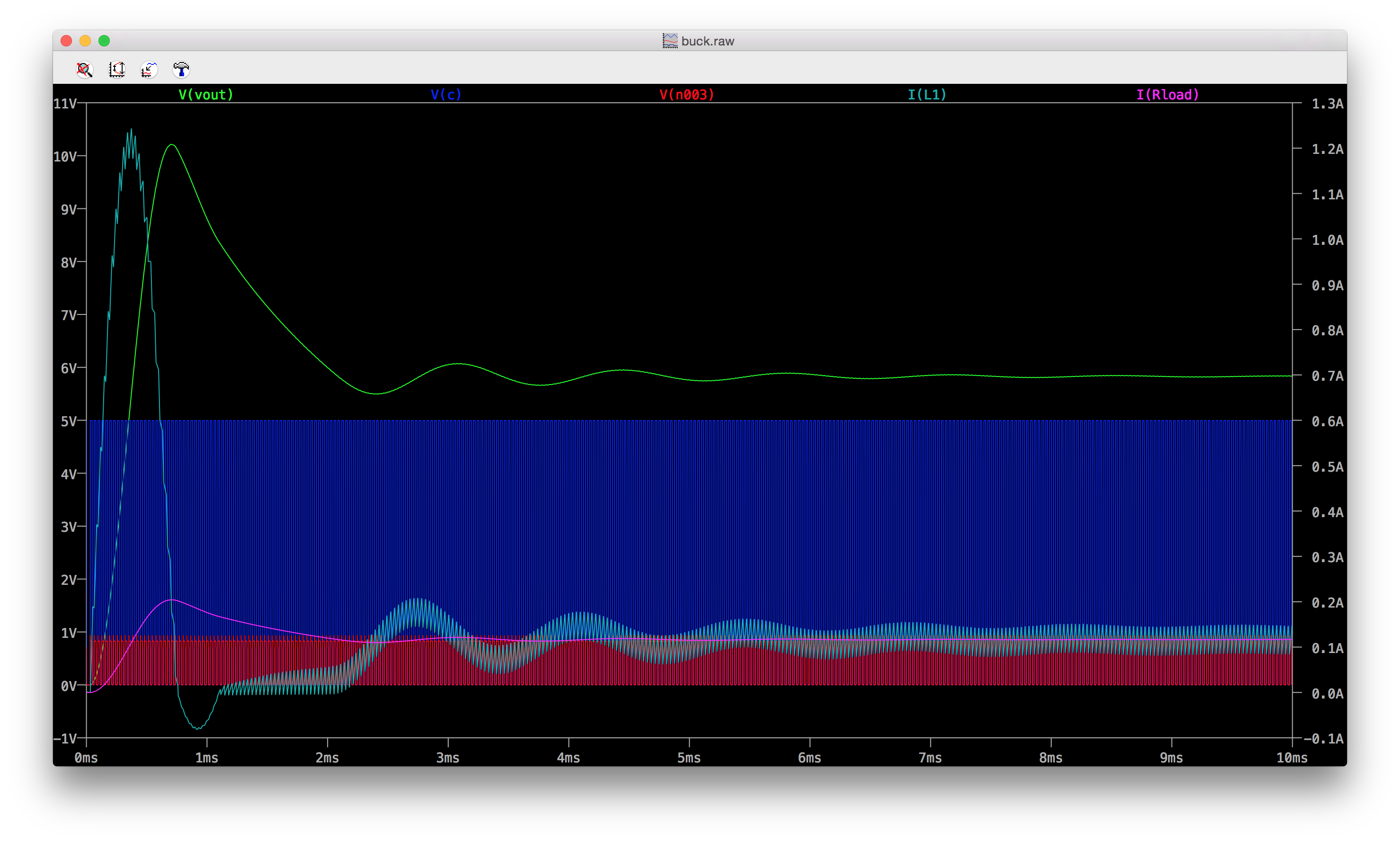
Note that this is far from simply 50% of Vin (9V). The variance is largely due to losses in the circuit and imperfect matching of components to the theoretical ideal.
Measurement - 50% Duty Cycle
With a duty cycle of approximately 50%, I’m measuring an output voltage (Vout) of ~5.8V with ~100mV ripple. That’s very close to the ltspice simulation.
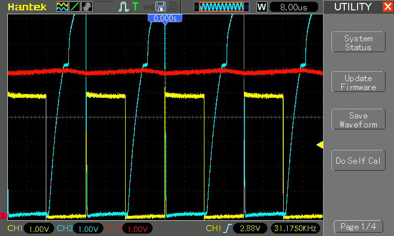
But both ltspice and actual measurements are far from the simple theory. Why?
It is a significant variation, but I believe it is primarily due to non-ideal components. e.g.
- I didn’t take into account ESR or other component losses
- response times are not instantaneous
- cross-over distortion when inductor voltage passes the output voltage
Conclusion?
- idealised theory can predict basic behaviour, but in order to calculate actual real-world performance it is essential to accommodate non-ideal component characteristics
- ltspice simulation is actually very good for predicting real-world performance
Next Steps / Improvements
-
High duty cycles will cause an initial undamped over-voltage spike. This can be avoided by gradually ramping up the duty cycle.
-
Add feedback control
-
perhaps replace the BJT with a MOSFET to reduce power loss in the switching stage
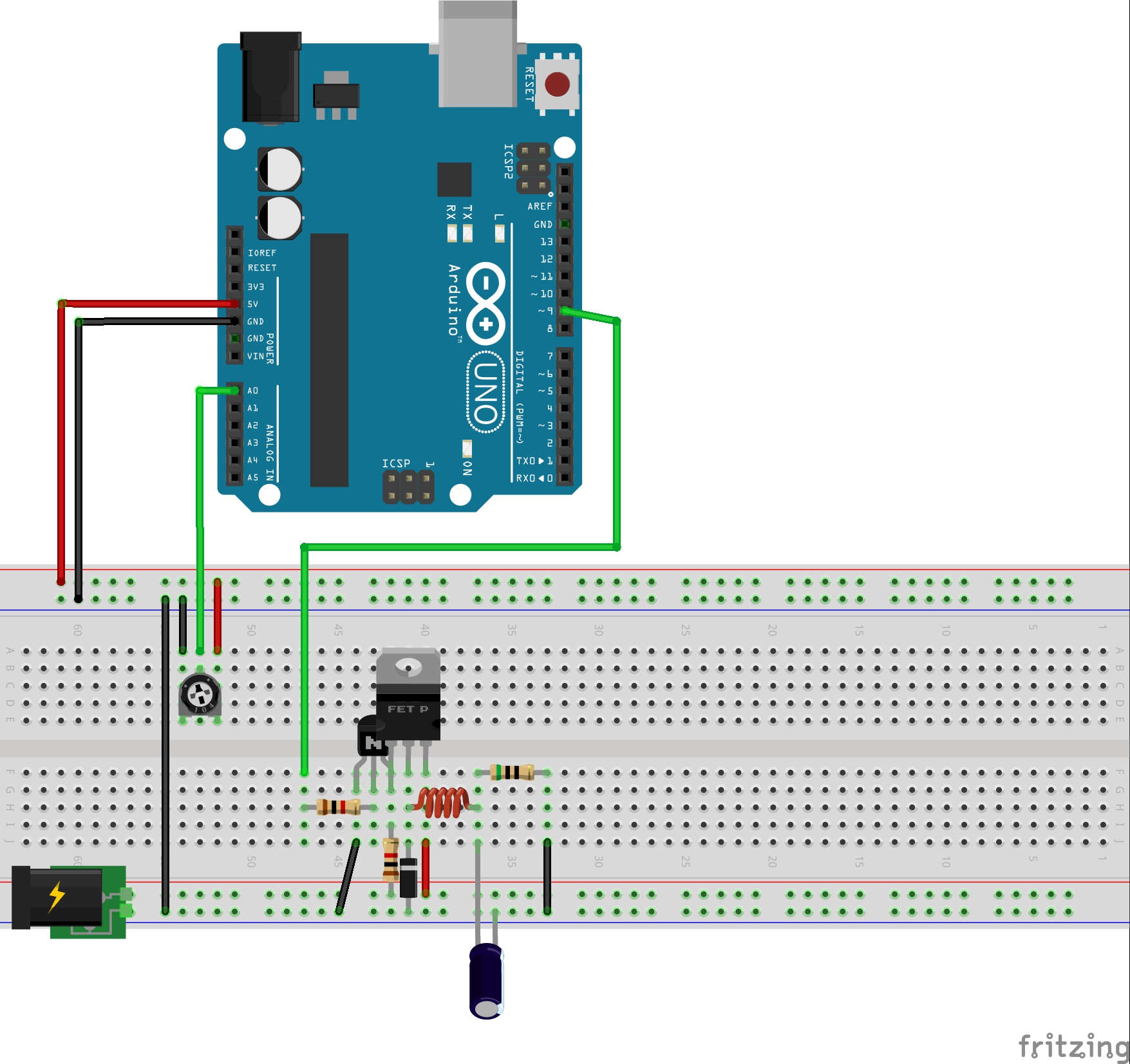
Construction

Credits and References
- Buck Converter - wikipedia
-
[DIY Buck Converter How to step down DC voltage efficiently](https://www.youtube.com/watch?v=m8rK9gU30v4) - GreatScott! - IRF9540 datasheet
- 2N3904 datasheet
- 1N5819 datasheet
- PwmFrequency
- analogRead()
- analogWrite()
- Method #3: Apply Over-voltage to I/O Pins
- Driving motors, lights, etc. from an Arduino output pin - Switching higher voltages
- Secrets of Arduino PWM
- Changing the Arduino PWM Frequency
- ..as mentioned on my blog
