
#389 Two-stage Common Emitter Amplifier
Designing a two-stage common-emitter BJT amplifier.

Notes
Cascading two common-emitter amplifiers is a means of achieving high voltage gain. Voltage gains from several hundred to several thousand are possible.
I’m going to try and noodle out a theoretical design of a two-stage Class A amplifier, and then test the actual performance. Do not take my calculations as gospel. My main sources for the theory were Electronic Principles by Albert Paul Malvino and a Multistage Transistor Amplifiers YouTube tutorial by The Offset Volt:
Designing a Single Stage for Gain ~ 10
| Parameter | Design/Spec Value |
|---|---|
| A (gain) | 10 |
| Vcc | 9V |
| Icq | 4mA |
| Vceq | 4.5V |
| ß (hFE) | 100 - 400 |
| hie | 1kΩ - 10kΩ |
| Vbe | 0.7V |
| RL | 2.2kΩ |
Also:
- r’e = hie/hFE = 10kΩ/400 = 25Ω
Calculate collector + emitter resistance for desired gain at the Q point
- Rc + Re = (Vcc - Vceq) / Icq
- Rc + Re = (9V - 4.5V)/4mA = 1.13kΩ
- assuming A ≅ Rc/Re
- Re = 1.13kΩ - Rc
- Re = 1.13kΩ/11 =100Ω
- Rc = 1.03kΩ, say 1kΩ
With the selected components, the theoretical gain is thus 10
Calculate the combined bias gang resistance
Base current at the q point
- Ib = 4mA / 100 = 0.04mA
Assume current through the gang at 10 x Ib as a rule of thumb to ensure “stiff” biasing i.e. 0.4 mA
So combined resistance = 22.5kΩ
Calculate the resistance of R1 and R2 components of the bias gang
Lower resistor R2:
voltage = 0.7 + Ic x Re = 1.1V
therefore R2 = 2.75kΩ say 3kΩ (standard value)
and therefore R1 = 19.5kΩ say 20kΩ (standard value)
Measure Performance - Single Stage

With 0.2V peak-peak 10kHz input, and Re = 100Ω (without emitter bypass), measured results:
- 0.2V input peak-peak
- 1.98V output peak-peak
- actual gain = 9.9
Conclusion: very close to design gain of 10, undistorted Class A performance.

Adjusting Single Stage Design with Bypass
I decided to add another 100Ω/100µF emitter bypass to the design, for a few reasons:
- it’s a common feature of such designs
- it provides negative feedback to stabilise for transistor variations (AC signals will vary the emitter resistance with inverse relationship to input/output differential, thus combating variation)
- reduces the gain a bit (so I can work with larger input signals in two-stage configuration while staying within the 9V supply limits)
Recalculating with this variation. DC characteristics are now:
- Re = 200Ω
- A ≅ Rc/Re = 1kΩ/200Ω = 5
combined base bias resistance should still be = 22.5kΩ
Lower resistor R2 is now:
voltage = 0.7 + Ic x Re = 1.5V
therefore R2 = 3.75kΩ say 3.6kΩ (standard value)
and therefore R1 = 18.9kΩ say 20kΩ (standard value)
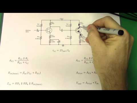
Calculating Two-stage Performance with RL load
With:
- component values duplicated the from the single-stage design for two stages
- with the extra
100Ω||100µFemitter bypass - and RL = 2.2kΩ
predicted performance calculated as follows:
DC analysis:
- Vb =
Vcc x Rb2/(Rb1 + Rb2)=9V x 3.6kΩ/(20kΩ + 3.6kΩ)= 1.37V - Ve =
Vb - 0.7V= 0.67V - Ie =
Ve/Re=0.67V/(200Ω)= 3.35mA - Ie ≅ Ic
- Vrc =
Ic x Rc=3.35mA x 1kΩ= 3.35V - Vce =
Vcc - (Vrc + Ve)=9V - (3.35V + 0.67V)= 4.98V - Isat =
Vcc/(Re + Rc)=9V/(200Ω + 1kΩ)= 7.5mA
Second stage:
- assuming thermal voltage VT = kT/q = 25 mV
- r’ej =
VT/Ie= 7.5Ω - A2 =
Rc||RL/(Re2 + r'ej)=1k||2.2kΩ/(100Ω + 7.5Ω)= 6.4 - Rin(base) =
ß(Re2 + r'ej)=100(100Ω + 7.5Ω)= 10.75kΩ - Zin =
Rin(base)||Rb1||Rb2=10.75kΩ||20kΩ||3.6kΩ= 2.38kΩ - A1 =
Rc1||Zin/(Re1 + r'ej)=1kΩ||2.38kΩ/(100Ω + 7.5Ω)= 6.55 - Total gain A = A1 A2 = 6.4 6.55 = 41.92
Assuming headroom for say 7V peak-peak, input limit would be around 0.17V peak-peak before clipping.
Measure Performance - Two Stage
With 0.1V peak-peak 10kHz input, and Re = 200Ω (with 100Ω/100µF bypass), measured results:
- 0.1V input peak-peak
- 3.88V output peak-peak
- actual gain = 38.8 = 31.8 dB
- error in the theoretical gain calc = 7%
Conclusion: predicted performance was quite close to the actual performance. And .. I have a functioning two-stage Class A amplifier to boot, with performance “in the ballpark” of the design.

Performance With an Ugly-style Build

With an ugly-style build, I see even better performance, and improved gain:
- 0.1V input peak-peak
- 4.32V output peak-peak
- actual gain = 43.2 = 32.71 dB
- error in the theoretical gain calc = -3%
More gain when built “properly”, this time overshooting estimates by a small margin (less than the tolerance on components).

At 400kHz, performance is maintained:

Construction


Testing on a breadboard:

Testing with an ugly-style build: