
#514 Subtraction Loop Counter Kit
Investigating a single-digit counter with configurable range and frequency built with 74HC192, CD4011 and CD4511 logic.

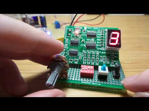
Here’s a quick demo..
Notes
Another cheap kit somehow found itself in my shopping cart(!) - this time a “Subtraction Loop Counter” featuring the 74HC192 Decade Counter.
Let’s take a look..
Kit
| Ref | Description | Qty |
|---|---|---|
| C1-C5 | 100nF 0603 capacitor | 5 |
| DS1 | 7-segment common cathode | 1 |
| IC1,IC2 | CD4011 SOP-14 Quad 2-Input NAND Buffered B Series Gate | 2 |
| IC3 | 74HC192 SOP-16 Decade Up/Down Counter with Clear | 1 |
| IC4 | CD4511 SOP-16 BCD-to-7 Segment Latch/Decoder/Driver | 1 |
| J1 | KF301-2P terminal | 1 |
| R1-R7 | 560Ω 0603 resistor | 7 |
| LED0 | 0805 red LED | 1 |
| R0 | 1kΩ 0805 resistor | 1 |
| R8 | 390kΩ 0805 resistor | 1 |
| R9-R14 | 10kΩ 0805 resistor | 6 |
| RP1 | 3.3MΩ potentiometer | 1 |
| S1-S6,TP1-TP9 | 2.54mm male pin headers | 15 |
| S1-S6 | jumper cap | 6 |


How it Works
First, a review of the ICs involved..
CD4011
The CD4011 quad 2-Input NAND gate is used for three purposes in the circuit:
- Schmitt oscillator, similar to that used in LEAP#465 MrBiJuT
- buffering and switching (enable/disable) the oscillator output
- combinatorial logic to trigger the counter reset
CD4511
The CD4511 is a BCD-to-7 Segment Latch/Decoder/Driver. Some key points:
- 4-bit BCD input
- only drives 7 segments (no decimal point)
- up to 25mA drive capability, which makes it flexible for driving different displays. but this also means that for 7-segment LED, current-limiting resistors are required.
Three control pins:
- LE (latch enable, active low). When low, segment output changes according to BCD input. When pulled high, holds current segment output state.
- BI (blanking, active low). When low, all segments off.
- LT (lamp test, active low). When low, all segments on.
| LE | Bl | LT | D | C | B | A | a | b | c | d | e | f | g | Display |
|---|---|---|---|---|---|---|---|---|---|---|---|---|---|---|
| x | x | 0 | x | x | x | x | 1 | 1 | 1 | 1 | 1 | 1 | 1 | 8 |
| x | 0 | 1 | x | x | x | x | 0 | 0 | 0 | 0 | 0 | 0 | 0 | (blank) |
| 1 | 1 | 1 | x | x | x | x | a0 | b0 | c0 | d0 | e0 | f0 | g0 | (hold last digit) |
| 0 | 1 | 1 | 0 | 0 | 0 | 0 | 1 | 1 | 1 | 1 | 1 | 1 | 0 | 0 |
| 0 | 1 | 1 | 0 | 0 | 0 | 1 | 1 | 1 | 1 | 1 | 1 | 1 | 0 | 1 |
| 0 | 1 | 1 | 0 | 0 | 1 | 0 | 1 | 1 | 1 | 1 | 1 | 1 | 0 | 2 |
| 0 | 1 | 1 | 0 | 0 | 1 | 1 | 1 | 1 | 1 | 1 | 1 | 1 | 0 | 3 |
| 0 | 1 | 1 | 0 | 1 | 0 | 0 | 1 | 1 | 1 | 1 | 1 | 1 | 0 | 4 |
| 0 | 1 | 1 | 0 | 1 | 0 | 1 | 1 | 1 | 1 | 1 | 1 | 1 | 0 | 5 |
| 0 | 1 | 1 | 0 | 1 | 1 | 0 | 1 | 1 | 1 | 1 | 1 | 1 | 0 | 6 |
| 0 | 1 | 1 | 0 | 1 | 1 | 1 | 1 | 1 | 1 | 1 | 1 | 1 | 0 | 7 |
| 0 | 1 | 1 | 1 | 0 | 0 | 0 | 1 | 1 | 1 | 1 | 1 | 1 | 0 | 8 |
| 0 | 1 | 1 | 1 | 0 | 0 | 1 | 1 | 1 | 1 | 1 | 1 | 1 | 0 | 9 |
| 0 | 1 | 1 | 1 | 0 | 1 | 0 | 0 | 0 | 0 | 0 | 0 | 0 | 0 | (blank) |
| 0 | 1 | 1 | 1 | 0 | 1 | 1 | 0 | 0 | 0 | 0 | 0 | 0 | 0 | (blank) |
| 0 | 1 | 1 | 1 | 1 | 0 | 0 | 0 | 0 | 0 | 0 | 0 | 0 | 0 | (blank) |
| 0 | 1 | 1 | 1 | 1 | 0 | 1 | 0 | 0 | 0 | 0 | 0 | 0 | 0 | (blank) |
| 0 | 1 | 1 | 1 | 1 | 1 | 0 | 0 | 0 | 0 | 0 | 0 | 0 | 0 | (blank) |
| 0 | 1 | 1 | 1 | 1 | 1 | 1 | 0 | 0 | 0 | 0 | 0 | 0 | 0 | (blank) |
74HC192
The 74HC192 Decade Up/Down Counter with Clear. Some key points:
- 4-bit BCD output ([MSB]:
Q3, Q2, Q1, Q0:[LSB]) - Terminal count up (TCU, active low), goes low when ‘9’ transitions to ‘0’ i.e. like carry out
- Terminal count down (TCD, active low), goes low when ‘0’ transitions to ‘9’ i.e. like reverse carry out
Control pins:
- clock up (CPU, rising edge trigger), counts 0-9, wraps back to 0
- clock down (CPD, rising edge trigger), counts 9-0, wraps back to 9
- master reset (MR, active high), resets output to 0
- asynchronous parallel load (PL, active low): loads 4-bit BCD preset from pins ([MSB]:
P3, P2, P1, P0:[LSB])
| Down (CPU) | Up (CPD) | Rest (MR) | Load (PL) | Function |
|---|---|---|---|---|
| ↑ | 1 | 0 | 1 | count up |
| 1 | ↑ | 0 | 1 | count down |
| x | x | 1 | x | reset |
| x | x | 0 | 0 | load preset |
Circuit Construction
Here’s my re-drawing of the circuit..


Principle of Operation
So, what is going on here?
The Oscillator
Four CD4011 NAND gates are used to implement a Schmitt oscillator providing the master clock for the circuit, similar to that used in LEAP#465 MrBiJuT. It includes a couple of tricks though:
- RP1 variable resistor provides clock frequency adjustment
- one NAND gate is used to buffer the clock output (measurable at TP1)
- another NAND gate is used for a clock enable/disable control based on the setting of switch (jumper) S1
- the final buffered & enabled clock (CLK) is measurable at TP1.
The Counter
The buffered & enabled clock output (CLK) feeds the count down pin (CPD) of the 74HC192. A few features of the 74HC192 are unused: count up; terminal count up and down.
The 74HC192 master reset can be toggled with switch (jumper) S2.
At this point, we have a free-running countdown timer (9-0) running at the frequency set by RP1.
7-segment display
The CD4511 BCD-to-7 Segment driver is simply connected to the 74HC192 output pins ([MSB]:Q3, Q2, Q1, Q0:[LSB]).
The CD4511 is permanently enabled; lamp test and blanking features are not used.
Individual 560Ω currently limiting resistors are used for each segment of the display.
Funky Combinatorial Parallel Load Logic
Finally, there’s some fun and games going on with the Parallel Load logic.
A flag (PSET) is set if a manually preset has been entered on the switches:
- preset pins ([MSB]:
P3, P2, P1, P0:[LSB]) are manually settable with switches (jumpers) S3-S6. Closed = low, open = high. - P0 and P3 are fed to one CD4011 NAND gate:
- P0 and P3 are pulled high by default
- P0 and P3 are only high in the digit
9 - For all other digits 0-8, one or both of P0 and P3 will be low
- The output (PSET) will be high if a digit 0-8 has been manually set on the switches S3-S6
A flag (IS9) is set if ‘9’ is currently being output on the 7-segment display:
- Q0 and Q3 are fed to one CD4011 NAND gate.
- Q0 and Q3 are only high in the digit
9 - The output (NOT9) will only be low if the digit
9is being displayed
- Q0 and Q3 are only high in the digit
- a second NAND gate is used to invert the value (IS9)
- this value will be high if
9is being displayed
- this value will be high if
The PSET and IS9 signals are fed to a final NAND gate:
- output will pull low when
9is being displayed, and a custom value has been set with the switches S3-S6. - this signal is fed to the 74HC192 asynchronous parallel load (PL, active low) pin.
- causing the 74HC192 to load the value from
P3, P2, P1, P0instead of continuing to count down from9
So the nett effect: the switches S3-S6 can be used to set the number 0-9 from which the countdown will start.
Sprucing Up the Build
I decided to replace the jumpers and variable resistor with some off-board components for an easier to use unit:
- replaced the dinky trim-pot with a full-sized variable resistor
- used a 4-point DIP switch for the P0-3 input
- used a switch for the clock enable S1
- used a pushbutton (momentary) for the 74HC192 master reset S2
- used an XH2.54 connector for power instead of the terminal block
The final result:
Some things that didn’t go so well
I started soldering the board with a hot air station, however this didn’t work so well as the PCB footprints for the ICs are not quite the right size - they are a little too wide so the IC feet barely touch the pads. Reverting to chisel tip iron and I made quick work of it.
The async parallel load inputs (P0-P3) are in LSB-first (on the left) order on the PCB. When I connected these to DIP switches, I didn’t think to re-orient the package so they could be entered in the most natural form: MSB-first with bit “on” oriented upwards. As it is, I need to enter the P* digits in reverse and upside down!