
#463 OpAmp Transconductance Amplifiers
Understanding transconductance amplifiers and how they can be realised with an op-amp, and testing both single and dual-supply transconductance circuits based on an LM741 op-amp.

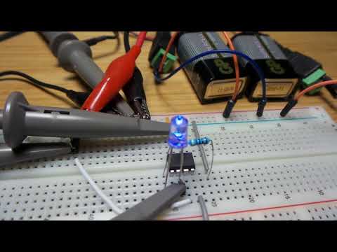
Here’s a quick demo
Notes
A Transconductance Amplifier is a circuit where differential input voltage produces a proportional output current. Specialised operational transconductance amplifiers such as the CA3080 used to be produced. The circuit here demonstrates how the effect can be achieved with a standard op-amp.
The circuit inspiration comes from the Engineer’s Mini-Notebook - Op Amp IC Circuits.
Circuit Theory
This is essentially just an application of a standard non-inverting amplified configuration:
        |\
Vin ----|+\
        |  \______ Vout
        |  /   |
      +-|-/    z
      | |/     z R1 (load)
      |        z
      |________|
               |
               z
               z R2
               z
              _|_
               =
With an ideal op-amp model, the inverting and non-inverting inputs must remain at the same potential, so the relationship between Vin and Vout is simply an application of the voltage divider equation:
Vin = Vout * R2 / (R1 + R2)
Which can be re-arranged to determine the voltage gain:
Vout = Vin (1 + R1/R2)
The output current Iout can likewise be expressed in two equations (Ohm’s Law), again assuming an ideal op-amp where the current at the inverting and non-inverting inputs is 0:
Iout = Vout/(R1 + R2)
Iout = Vin/R2
And that last line is the essence of a transconductance amplifier: the output current is a function of input voltage.
Dual-Supply Circuit Design
I’m using a venerable LM741 op-amp for this circuit. It is pretty terrible by modern standards, but makes an interesting case study for applying theory in the real world.
The analysis above is fine as long as the op-amp has enough headroom to cater for the full range of voltage swings. The easiest and classic way to achieve this is to power the op-amp with dual supply rails. In this case, I’ll use two 9V batteries in series to provide +/- 9V supply around “ground” at 0V.
Since R1 can be considered the “load”; I am substituting this with a 1kΩ resistor and a blue LED. The effect I am looking for is varaible LED current by adjusting Vin.
Vin is adjusted with a 10kΩ pot:


A few results from manual testing, with Vcc = +9.84, Vee = -9.88. Since the 741 is not rail-to-rail, the top-end of the range is truncated, however thanks to the split supploy, it is able to deliver a true 0 output (but the whole negative voltage range is wasted)
| Vin | V(-) | Vout | Iout |
|---|---|---|---|
| 0 | 0 | 2.31 | 0 |
| 4.41 | 4.41 | 8.1 | 4.4mA |
| 9.84 | 5.18 | 9.04 | 5.18mA |
Replacing the 10kΩ pot with a signal generator (10kHz sine wave), and hooking the circuit up to a scope provides a bit more insight. Here’s what it looks like on the bench:

For the scope traces below, channel connections are as follow (also as annotated in the schematic):
- CH1 (yellow) - Vin
- CH2 (blue) - Vout; note the vertical scale may be different to fit the signal on the chart
- CH3 (red) - V(-), negative op-amp input and LED cathode (should be the same as Vin until the op-amp starts distorting/clipping)
- CH4 (green) - “virtual” ground
With full 18V peak-peak deflection on the input signal, we see the operating range as a relatively small region:

Adjusting (roughly) the input signal to deliver the maximum undistorted output range, we find the limits of the 741 design.
The trace below shows a relatively clean, proportional and equal output signal, which would in turn deliver linearly proportional output current (Iout). The input signal is 5.1V peak-peak with a 2.7V offset, in other words oscillating from 0.2V to 5.25V.
A nice clean result, but for an 18V power supply, that’s a pretty poor operating range!

If the input falls below 0V, Vout swings hard to the negative rail, as shown on the following trace (note that traces are offset -2V):

Single-Supply Circuit Design
Single-supply op-amp configurations may not be better but they can certainly be more convenient (single supply meaning: drop the negative rail and operate with just ground and a positive voltage supply).
The 741 is not a great chip to use in a single-supply configuration due to it’s pretty horribly upper and lower limits - According to the 741 datasheet, with a +/-20V supply, the output voltage may swing as little as +/-15V.
But let’s try.
Since I still want to be able to turn the LED/output current completely off, I don’t want to simply replace Vee with a ground connection.
As a simple solution, I’ve used a series of diode drops to create a “virtual ground”. Adding four 1N4148 diodes (for a drop of about 1.95V) just about does the trick. Alternatively a 3.3V 1N4728 zener diode also works.


With full 9V peak-peak deflection on the input signal, we see the operating range as a relatively small region. This trace has all signals offset by -2V so they fit in the screen.

Adjusting (roughly) the input signal to deliver the maximum undistorted output range results in an input signal at 3.5V peak-peak, with a 4.0V offset, in other words oscillating from 2.25V to 5.75V.

Conclusion
A non-inverting op-amp configuration is an effective means of simulating a transconductance amplifier, however there are limitations particualrly in terms of the operational voltage range that can be achieved.
Credits and References
- LM741 Datasheet
- 1N4148 Datasheet
- 1N4728 Datasheet
- Engineer’s Mini-Notebook - Op Amp IC Circuits - p14 Transconductance Amplifier
- Operational transconductance amplifier - wikipedia