
#663 3-Digit LCD Panel
Testing a small 3V, 3-digit LCD panel with an example of driving the multiplexed LCD (1/4 duty, 1/2 bias) with an Arduino/ATmega328 sketch.

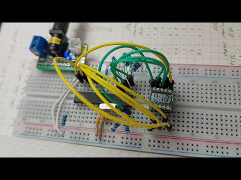
Here’s a quick demo..
Notes
I found this small 10PIN TN Positive 3-Digits Segment LCD Panel 3.0V Digital Tube Display from a seller on aliexpress.
The part is multiplexed liquid crystal display that must be driven at 1/4 duty, 1/2 bias.
Part Specifications
The main technical parameters of the product:
- Dimensions: 11.5*10.3mm
- Conductive glass thickness: 0.7mm
- Minimum pixel gap: 10µm
- Duty ratio: 1/4 duty 1/2 bias
- Voltage: 3.0V
- Working temperature: -0˚C to +50˚C
- Viewing direction: 6 points
- Twisted Nematic (TN) type viewing range 60 degrees. Reflection
- Connection: 10 pin, dual inline with 2mm pin pitch

Since the module has a 2mm pin pitch, I squeezed it onto a DIP10 adapter board for use on a breadboard..

Pin Functions
| Pin | 1 | 2 | 3 | 4 | 5 | 6 |
|---|---|---|---|---|---|---|
| 10 - COM1 | 3D | 2D | 1D | |||
| 9 - COM2 | 3C | 3E | 2C | 2E | 1C | 1E |
| 8 - COM3 | 3B | 3G | 2B | 2G | 1B | 1G |
| 7 - COM4 | 3A | 3F | 2A | 2F | 1A | 1F |
Multiplexed LCD Control
LCD panels like this one must be driven directly. Each LCD segment must be driven with an AC signal, as the are capacitive in nature.
- 1/2 bias: means the COMmon signals are driven at 3 levels: +VCC, VCC/2, and 0
- 1/4 duty: meaning we have 4 COMmon signals, each take 1/4 of the duty cycle
The basic mechanism:
- COM1-4 are normally at VCC/2
- COM1-4 each in turn will clock to VCC, then 0 and back to VCC/2
- SEGMENT pins will all clock in phase to be “off”, constantly feeding the segments an AC signal between +VCC/2 and -VCC/2
- to turn segment “on”, it is inversely clocked during the corresponding common clocking cycle. this will pulse the segment with an AC signal between +VCC and -VCC
Multiplexed Digit Encoding
Digit segments are “lettered” in the conventional order:
|-a-|
f   b
|-g-|
e   c
|-d-|
Each digit is encoded with two segment lines (“d0, d1”) over the 4 COM states. So the encoding table is as follows:
| com:  |  COM 4  |  COM 3  |  COM 2  |  COM 1  |
|-------|----|----|----|----|----|----|----|----|
| line: | d1 | d0 | d1 | d0 | d1 | d0 | d1 | d0 |
|-------|----|----|----|----|----|----|----|----|
| seg:  | f  | a  | g  | b  | e  | c  | d  | -  |
|-------|----|----|----|----|----|----|----|----|
|    0: | 1  | 1  | 0  | 1  | 1  | 1  | 1  | 0  |
|    1: | 0  | 0  | 0  | 1  | 0  | 1  | 0  | 0  |
|    2: | 0  | 1  | 1  | 1  | 1  | 0  | 1  | 0  |
|    3: | 0  | 1  | 1  | 1  | 0  | 1  | 1  | 0  |
|    4: | 1  | 0  | 1  | 1  | 0  | 1  | 0  | 0  |
|    5: | 1  | 1  | 1  | 0  | 0  | 1  | 1  | 0  |
|    6: | 1  | 1  | 1  | 0  | 1  | 1  | 1  | 0  |
|    7: | 0  | 1  | 0  | 1  | 0  | 1  | 0  | 0  |
|    8: | 1  | 1  | 1  | 1  | 1  | 1  | 1  | 0  |
|    9: | 1  | 1  | 1  | 1  | 0  | 1  | 0  | 0  |
|-------|----|----|----|----|----|----|----|----|
AVR Arduino/ATmega328 Raw Driver Design
For testing purposes, I’ll be using an ATmega328P with a program that directly implements the necessary LCD control. I’ll run the chip at 3V to avoid level-shifting.
To simplify programming and allow for bulk GPIO operations, I’ve aligned the pin connections with two GPIO ports - COM pins on port PB, and SEG pins on PC:
| Port | Arduino Pin | ATmega328 Pin | LCD pin |
|---|---|---|---|
| PB0 | 8 | 14 | COM1 |
| PB1 | 9 | 15 | COM2 |
| PB2 | 10 | 16 | COM3 |
| PB3 | 11 | 17 | COM4 |
| PC0 | 14/A0 | 23 | SEG1 |
| PC1 | 15/A1 | 24 | SEG2 |
| PC2 | 16/A2 | 25 | SEG3 |
| PC3 | 17/A3 | 26 | SEG4 |
| PC4 | 18/A4 | 27 | SEG5 |
| PC5 | 19/A5 | 28 | SEG6 |
For demonstration purposes, I’ll just have the code run a simple seconds timer.
Algorithm Outline
There are basically two timing loops:
- per second, increment the number to display
- cycle the COM line at > 30 Hz to prevent flicker
The COM refresh loop is an 8-stage cycle, where COM pins toggle between (H)igh, (L)ow or High-(Z):
| step | COM1 | COM2 | COM3 | COM4 |
|---|---|---|---|---|
| 0 | H | Z | Z | Z |
| 1 | L | Z | Z | Z |
| 2 | Z | H | Z | Z |
| 3 | Z | L | Z | Z |
| 4 | Z | Z | H | Z |
| 5 | Z | Z | L | Z |
| 6 | Z | Z | Z | H |
| 7 | Z | Z | Z | L |
When setting the number to display:
- update the 8 SEG encoding patterns for the 8 COM steps
For each COM step:
- increment/reset the step counter
- set COM port state (output / high Z)
- write COM port output value
Simple (Unoptimised) Approach
All the GPIO operations can be performed with standard pinMode digitalWrite
The Simple.ino sketch implements this simple approach. It runs at around 40Hz full duty cycle. Here is a scope trace of an example COM/SEG pair:
- COM1 - CH1 Yellow
- SEG6 - CH2 Blue

Clever (Optimised) Approach
The LCD refresh is fully determined by the register configuration of the DDRx and PORTx registers.
So instead of using the standard AVR functions, it is much easier and efficient (though perhaps a little more opaque) to simply update the 4 registers of concern: DDRB, DDRC, PORTB, PORTC.
I haven’t implemented this version (yet).
Circuit Design


Credits and References
- 10PIN TN Positive 3-Digits Segment LCD Panel 3.0V Digital Tube Display - aliexpress
- Multiplex Drive and Bias of LCD Technology
- How an LCD controller drives an LCD glass
- Direct LCD drive by AVR GPIO
- LCD Fundamentals and the LCD Driver Module of 8-Bit PIC Microcontrollers
- pinMode function
- digitalWrite function
- AVR register configuration