
#562 1-bit Register
Building a basic manually controlled 1-bit register that demonstrates the key features of a digital register.

Here’s a quick demo..
Notes
Another micro-project inspired by Ben Eater’s descent into digital logic. This is a quick build of a basic 1-bit register using 7000-series CMOS logic that demonstrates the key features we require in a functional digital register:
- input loaded only when a “load enable” signal is present
- latching of the value read into the register
- tri-state output control: high, low, or high-impedance (high Z)
The ideas demonstrated here are covered in depth in one of Ben Eater’s videos from his 8-bit computer series, “Designing and building a 1-bit register - 8 bit register - Part 3”:
Logic Design
The basic concepts:
- A D latch provides the central storage of current state
- The load signal is combined with the data signal (with inverter, AND and Or gates) such that:
- when load is low, the current output is fed back as the current input (no change in output state)
- when load is high, the data value is presented as the input data for the D latch
- a tri-state output ensures:
- the D latch output (Q) is only present on the final output when output is enabled
- when output is disabled, the output is high impedance

NB: I sketched this in logic.ly (unsaved - still looking for a good online digital logic editor)
Truth Table
| Load | Data | Output Enable | Clock | Output (Q) |
|---|---|---|---|---|
| 0 | 0 | 1 | ↑ | Z |
| 0 | 1 | 1 | ↑ | Z |
| 1 | 0 | 1 | ↑ | Z |
| 1 | 1 | 1 | ↑ | Z |
| 0 | 0 | 0 | ↑ | Q₀ |
| 0 | 1 | 0 | ↑ | Q₀ |
| 1 | 0 | 0 | ↑ | 0 |
| 1 | 1 | 0 | ↑ | 1 |
Legend/Notes:
- 0 - logical 0 (low)
- 0 - logical 1 (high)
- Q₀ - output stays the same
- ↑ - rising edge
- Z - high impedance
- Output Enable is active low
Construction
The design can be realised with fundamental building blocks from the 7000-series CMOS series:
- 74LS04 - provides the inverter (only 1 or 8 used)
- 74LS08 - provides the AND gates (only 2 of 4 used)
- 74LS32 - provides the OR gates (only 1 of 4 used)
- 74LS374 - provides the D lath and tri-state output (only 1 of 8 used)
I’ve drawn the schematic for the circuit here (EasyEDA).

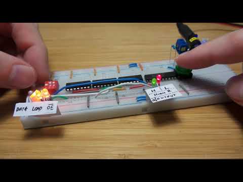
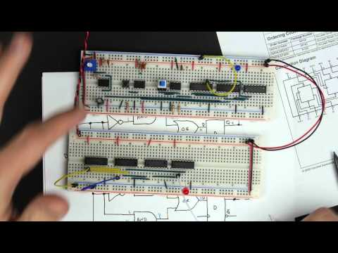
I built the circuit on a bread board, with additional components for manual control:
- a 3 switch DIP switch unit implements Data, Load, and Output Enable. Each has an associated pull-down resistor and LED indicator
- a push-button with pull-down resistor provides a manual clock input
- the final output is wired to 2 LEDs with current-limiting resistors:
- when output HIGH, the green LED is lit
- when output LOW, the red LED is lit
- when output is high Z, both red and green LEDs are lit, but a little dimly
Credits and References
- 74LS04 Datasheet - Hex Inverting Gates
- 74LS08 Datasheet - Quad 2-Input AND Gates
- 74LS32 Datasheet - Quad 2-Input OR Gate
- 74LS374 Datasheet - 3-STATE Octal D-Type Edge-Triggered Flip-Flops