
#371 BJT Common-Emitter Amplifier
All about BJT common-emitter amplifier biasing and class of operation.

Notes
Time to revisit the basics of biasing a bipolar junction transistor in an NPN common-emitter amplifier configuration. I am inspired once again by one of w2aew’s excellent videos - this time #113: Basics of Transistor bias point and the class of amplifier operation.
The Common Emitter Amplifier
The common emitter (CE) amplifier arrangement refers to cases where the transistor emitter shares a connection to both the input and output signal (ignoring resistors that may be in the path).
CE amplifiers generally have:
- “modest” gain
- input impedance of a few kΩ
- inverted output
Biasing the amplifier aims to place the transistor somewhere in the active region, between cut-off and saturation. Specifically, this means setting the:
- DC operating point (Quiescent Point) with no applied input signal
- gain
Together these will determine the class of operation.
Class of Operation
| Class | Amplifies | Typical Applications |
|---|---|---|
| A | entire waveform without distortion (360˚) | high fidelity linear audio amplifiers |
| B | half cycle (180˚) | RF |
| C | less than half cycle (< 180˚) | oscillator circuits |
| AB | between half and full cycle (180˚-360˚) | audio power amplifiers |
It may seem like class A should always be preferred, but that is not true as it is also the most power hungry.
Design Steps
An approach and example for selecting values for a simple CE amplifier:
1. Choose the operating requirements
VCC = 5VA = 2(low gain)- quiescent current
Icq = 4mA(a value to keep power dissipation low) - quiescent voltage
Vceq = 2.5V(rule of thumb - about half VCC) - assume
ß (hFE) = 150(or lookup the datasheet) - assume
Vbe = 0.7V(or lookup the datasheet)
2. calculate collector + emitter resistance for desired gain at the Q point
Aiming for Vcc/2
- Rc + Re = (5V/2) / 4mA = 625Ω
3. calculate Rc and Re for desired gain
A ≅ Rc/ReRe = 625Ω - RcRc = 2 x 625Ω - 2 x RcRc = 2/3 x 625ΩRe = 1/3 x 625Ω = 208Ωsay 220Ω (standard value)Rc = 416Ω, say 470Ω (standard value)
4. calculate base current at the q point
Ib = 4mA / 150= 0.02667mA
5. calculate the combined bias gang resistance
assume current through the gang at 10 x Ib as a rule of thumb to ensure “stiff” biasing i.e. 0.2667mA
so combined resistance = 5V/0.2667mA = 18.8kΩ
6. calculate the resistance of R1 and R2 components of the bias gang
Lower resistor R2:
voltage = 0.7 + Ic x Re = 1.58V
therefore R2 = 5924Ω so choose 5 kΩ (standard value)
and therefore R1 = 13.8kΩ so choose 12kΩ (standard value)
7. review input limits
with a design gain of 2, and assuming we have say 4V peak-to-peak headroom around the 2.5V quiescent point, we should be able to handle signals of 2V peak-to-peak
That’s all pretty theoretical and assumes nothing much about the transistor performance (except for ß), so let’s see how it works in practice.
With a 10kz 0.8V peak-to-peak input, here’s how I see the output on a scope.
- CH1: input (AC coupled)
- CH2: output (AC coupled)

That’s pretty spot-on!
- input bias point is around 1.48V, actually measures 816mV peak-to-peak on the scope
- output is centered on 3.12 V, and measures 1.68V peak-to-peak
- so an actual gain of 2.06
- no distortion - nice clean class A amplification
Bias Class Testing
Borrowing heavily from w2aew’s tutorial, I’ve wired up a circuit to demonstrate the different classes of operation by switching R1.
Class B Operation
For class B (half waveform), we want the bias point to sit at around 0.6 to 0.7 V (the Vbe voltage drop).
Keeping R2 at 5kΩ, we should switch R1 to around 37kΩ to scale the bias point.
Here’s the result. Just about perfect.
- CH1: input (DC coupled)
- CH2: output (DC coupled and offset -5V)

Note: I didn’t scale R1 and R2 back accordingly to keep the current through the bias gang above 10 x Ib.
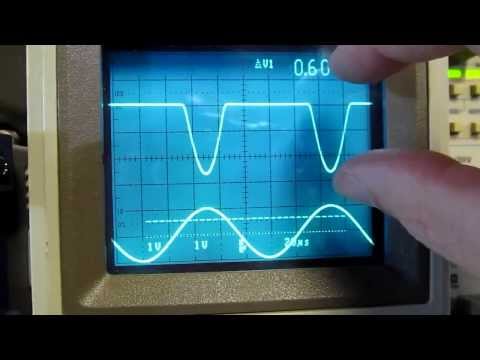
Class C Operation
For class C (less that half waveform), I just increased and adjusted R1 by trial and error to get a minimal peak. Finally settled at R1 ~80kΩ.
- CH1: input (DC coupled)
- CH2: output (DC coupled and offset -5V)

Note: I didn’t scale R1 and R2 back accordingly to keep the current through the bias gang above 10 x Ib.
Input and Output Impedance Calculation
Input impedance:
- the input sees R1, R2 and the impedance of the base (about 33k, hFE * Re) in parallel, so around 5kΩ
- the input capacitor combines with the resistance in a high-pass filter, C1 should be chosen to ensure input frequencies are far above the 3dB point
Output impedance:
- just Rc in parallel with the impedance looking into the collector, which is “very large”
- so Rc is a good approximation i.e. 470Ω in this case
Bypassed Emitter Resistor and Other Refinements
It is common to see a bypass capacitor in parallel with the emitter resistor. This improves stability of a grounded emitter amplifier i.e. when Re is low to maximise gain. No calculations or experiments for that here yet.
In practice, biasing can get a whole lot more complex, and “real” amplifier circuits may involve multiple transistors, either in Darlington or push-pull configurations, with biasing tricks that involve diodes to fix particular voltage drops.
Breadboard Construction
I first breadboarded this experiment, and used an external function generator for the 10kHz input signal.


Ugly Demo Board
Just for fun, I mounted the circuit ugly style on some discarded packaging. A jumper is used to select from the pre-set Class A, B, C configurations.
Under test, performs just fine..


Credits and References
- “Hands-On Radio: The Common Emitter Amplifier” by Ward Silver, NØAX. Feb 2003 QST
- The Art of Electronics, 2nd Edition - 2.13 Biasing the common-emitter amplifier, p84.
- #113: Basics of Transistor bias point and the class of amplifier operation - w2aew
- w2aew’s notes
- Common Emitter Amplifiers - electronics-tutorials
- Class AB Amplifier - electronics-tutorials
- Class A Power Amplifiers - learnabout-electronics
- Class B Power Amplifiers - learnabout-electronics
- Class C Power Amplifiers - learnabout-electronics
- Class AB Power Amplifiers - learnabout-electronics
- Common Emitter Mode - learnabout-electronics
- 2N3904 datasheet
- ..as mentioned on my blog