
#506 Learning PCBmodE
Learning how to use Boldport PCBmodE design software with an example of making a simple 555 timer LED blinky PCB.

Notes
I’ve long been aware that Saar uses his own EDA software called PCBmodE for all the Boldport designs. It is open source but this is the first time I’ve made a serious effort to learn how it works and try to build a PCB with it.
The following are my notes on getting up and running with PCBmodE, culminating in the design of a new board based on a simple 555 timer circuit.
Installing PCBmodE
See the setup docs. I have a Mac with all the pre-requisites already installed, so I just needed to clone the PCBmodE repo and run setup (in a dedicated Python 2.7 virtual environment)..
$ git clone https://github.com/boldport/pcbmode.git
$ virtualenv venv
$ source venv/bin/activate
$ cd pcbmode
$ python setup.py install
Folder structure
I’m running all my PCBmodE experiments from this folder. It has the following structure:
$ ls -1
README.md           # these notes
assets              # assets for these notes
boards              # <-- folder for project boards
generate_blinky.py  # <-- blinky board generator
pcbmode             # <-- cloned repo
python-pcbmode-zero # <-- cloned repo
venv                # <-- python virtual environment
Compiling an Example Board: widlar
Boldport publish all the project design files. I’ve chosen the widlar project for a quick test:
$ git clone https://github.com/boldport/widlar.git boards/widlar
$ pcbmode -b widlar -m
-- Processing PCBmodE's configuration file
-- Processing board's configuration file
-- Creating board
 * Placing components:LED1 R4 R6 LED2 R1 R2 R3 T6 T2 R8 J1 J2 T3 R7 R5 µA723 C3 C2 C1 C4
 * Placing routes
 * Placing vias
 * Placing shapes
 * Placing documentation
 * Placing drill index
 * Placing layer index
-- Done!
This generates two build files:
boards/widlar/build/paths_db.jsonboards/widlar/build/widlar.svg
Loading with inkscape boards/widlar/build/widlar.svg to inspect:

Generating production files:
$ pcbmode -b widlar --fab
-- Processing PCBmodE's configuration file
-- Processing board's configuration file
-- Creating Gerbers
-- Creating excellon drill file
-- Done!
This generates gerber files in a default boards/widlar/build/production folder:
widlar_rev_A_bottom_conductor.ger
widlar_rev_A_bottom_silkscreen.ger
widlar_rev_A_bottom_soldermask.ger
widlar_rev_A_bottom_solderpaste.ger
widlar_rev_A_documentation.ger
widlar_rev_A_drills.txt
widlar_rev_A_outline.ger
widlar_rev_A_top_conductor.ger
widlar_rev_A_top_silkscreen.ger
widlar_rev_A_top_soldermask.ger
widlar_rev_A_top_solderpaste.ger
I zipped up the production folder and uploaded to a randomly chosen viewer - www.gerber-viewer.com - and it renders thus:

Generating for OSHPark
I tried uploading the default production files to OSHPark only to discover they don’t match the required Naming Patterns.
A quick look at the source, discovered there’s an ‘oshpark’ fab option. Let’s try that:
$ pcbmode -b widlar --fab oshpark
-- Processing PCBmodE's configuration file
-- Processing board's configuration file
-- Creating Gerbers
-- Creating excellon drill file
-- Done!
This generates gerber files in the boards/widlar/build/production folder:
widlar_rev_A_bottom_conductor.GBL
widlar_rev_A_bottom_silkscreen.GBO
widlar_rev_A_bottom_soldermask.GBS
widlar_rev_A_bottom_solderpaste.GBP
widlar_rev_A_documentation.GBR
widlar_rev_A_drills.XLN
widlar_rev_A_outline.GKO
widlar_rev_A_top_conductor.GTL
widlar_rev_A_top_silkscreen.GTO
widlar_rev_A_top_soldermask.GTS
widlar_rev_A_top_solderpaste.GTP
These uploaded to OSHpark without issue - you can see the generated project here.

PCBmodE Workflow
I learned (the hard way) that if you don’t read the workflow docs, then figuring out why and how to use PCBmodE will be a trial of massive fail. It is nothing like any other EDA tool I’ve ever come across!
In essence, design is an iterative processes shuttling between the JSON definitions and the SVG representation:
JSON board definition ->
   compile with PCBmodE to SVG (`pcbmode -b board -m`) ->
   view/edit the SVG ->
   feedback any changes into the JSON files and repeat
When the design is “ready”, generate production files using PCBmodE (pcbmode -b board --fab).
Saar’s process/design tips (compiled from comments in discord):
- sketch in my notebook while anticipating how that concept will be translated into physical form.
- It’s possible that I flesh-out 3 or 4 concepts in my notebook. Each can take an hour to make… it’s not quick.
- With the later sketches I will try to factor in the dimensional constraints that I know will affect the physical design.
- Then I mock-up in Inkscape. I’ll draw shapes 1:1 and often bring in footprints to give me perspective and context.
- I try to nail down the shapes (mainly outline) before actually starting to design the PCB with PCBmodE.
- Like @Ben B says, I have a shapes.svg in the repo where I create all the shapes I need, including intermediates so I can go backwards if I need to make changes.
Tutorial: PCBmodE Blinky
A PCBmodE tutorial using a simple 555 timer LED blinky circuit as a case study.
NB: the hello-solder tutorial mentioned in the docs appears to need some updating to be compatible with the current PCBmodE software. In particular, it seems the shapes structure out-dated.
A Simple Circuit
For a simple tutorial, I’m building a standard astable 555 timer circuit with an LED on the output. The circuit will flash at about 1Hz with R1=10kΩ, R2=330kΩ, C1=2.2µF.

Bootstrap with PCBmodEZero
PCBmodEZero is an experimental Python frontend to PCBmodE. Installation:
pip install pcbmodezero
I decided to use PCBmodEZero in generate_blinky.py to generate an initial placement of components.
$ python generate_blinky.py
-- Processing PCBmodE's configuration file
-- Processing board's configuration file
-- Creating board
 * Placing components:LED1 R1 R2 R3 J1 C2 IC1 C1
 * Placing routes
 * Placing vias
 * Placing shapes
 * Placing documentation
 * Placing drill index
 * Placing layer index
-- Creating Gerbers
-- Creating excellon drill file
-- Creating PNGs
 * Generating PNGs for each layer of the board
...
-- Done!
The script generates an initial board definition and SVG in board/blinky.
This worked pretty well, although I was unable to get it to generate routing with connect_pins.
Routing, Outline and Finishing Touches
To finalise the board, I used the standard hand-crafted PCBmodE flow:
- view/edit the SVG with inkscape
- manually feed changes back into the board files (
blinky.json,blinky_routing.json) - regenerate with
pcbmode -b blinky -m
After a few iterations, I had a design that was at least electrically complete and demonstrates a few of the boldport hallmarks such as wiggly traces and irregular outlines:

Generating Production Files
I shopped around the various PCB houses, and it turns out that OSHpark is happily the cheapest for this order (due to free shipping).
Generating the production files for OSHpark:
pcbmode -b blinky --fab oshpark
After checking the board in the gerber viewer and double-checking the circuit, I’ve put my order in. The project can be found here on OSHpark.

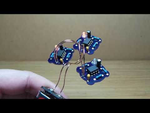
UPDATE: the boards have arrived thanks to some speedy shipping from OSHPark. Electrically, they check out perfectly..

I built all three of the boards and decided to mount them on a little wire sculpture and a 9V battery adapter.
The actual components I used:
| Part | Description |
|---|---|
| R1 | 10kΩ |
| R2 | 330kΩ |
| C1 | 2.2µF |
| C2 | 100nF |
| IC1 | NE555 |
| LED1 | 3mm orange LED |


Here’s a quick demo of the boards in action..
Conclusions
Well, my first PCBmodE boards turned out just fine, at least I was able to produce something that works - hardly an expert yet. Some observations on the PCBmodE design process so far:
- once one has all the components roughly laid out, designing in inkscape is wonderfully freeing compared to traditional EDA tools
- but the process for feeding changes back into the board design is a bit laborious - unless one is disciplined I can image it easily becoming a hot mess
- it’s important to remember to covert all strokes to paths (Path menu in inkscape) before trying to put them back into the PCBmodE JSON files
With small boards, the process gets you up and personal with the intricacies of the board design - which is great if one is trying to produce something startling and unique. I don’t know how I’d go with much larger designs without added tool help.
So far my bottom line: this is a really liberating way to build boards, especially when you want to get creative. I can’t help thinking that improvements in tooling (especially WYSIWYG component selection and automated feedback of design changes) would make for something really powerful that I’d want to use for even regular designs.
More comments perhaps once I’ve done another design or two..
Credits and References
- PCBmodE - on GitHub
- PCBmodE docs
- PCBmodEZero
- OSHpark